Maksutov- Cassegrain (Mak-Cass) Reflector
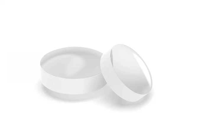
A catadioptric design using a thick, deeply curved spherical meniscus lens as its front corrector instead of a Schmidt plate's thin aspheric figure — trading a longer thermal cool-down time and heavier front element for a corrector that's fabricated using only simple, well-understood spherical grinding and testing methods, and prized for exceptionally high planetary and lunar contrast.
Corrector
Thick spherical meniscus lens
Primary mirror
Spherical
Typical f-ratio
f/12 – f/15
Secondary mount
Aluminized spot on corrector
Overview
- Uses a thick, strongly curved meniscus (crescent-shaped) lens as the front corrector, whose two surfaces are both simple spheres — unlike the Schmidt corrector's subtle non-spherical figure — with the meniscus's specific combination of curvatures and glass thickness calculated to cancel the spherical primary's aberration
- Because both of the meniscus corrector's surfaces are true spheres, they can be ground and tested with the same straightforward, well-established methods used for any spherical mirror or lens — avoiding the specialized aspheric-figuring techniques a Schmidt corrector demands, which is the design's core manufacturing advantage
- The secondary mirror is typically a small aluminized spot formed directly on the meniscus's inner (concave) surface, similar in principle to an SCT's corrector-mounted secondary
- The trade-off for spherical-only fabrication simplicity is the meniscus's substantial glass thickness and mass compared to a Schmidt plate, which both adds weight to the front of the tube and means more glass volume needs to thermally stabilize to ambient temperature before the telescope reaches peak sharpness — a longer cool-down process than a comparable SCT or Newtonian
- Typically built at longer focal ratios (f/12-f/15) than a standard SCT, narrowing the field of view but often delivering exceptionally high contrast for planetary and lunar detail, a characteristic Maksutov owners frequently prize
Key Features
All-spherical optical surfaces
Every optical surface in the system — both meniscus faces, the primary, and the secondary — is a simple sphere, simplifying fabrication and testing versus a Schmidt corrector's aspheric figure.
Exceptional planetary contrast
Delivers spherical-aberration-free, high-contrast images at the exact field center — well suited to planetary observation where the target sits centered in the field.
Longer thermal cool-down
The thick meniscus corrector's substantial glass mass takes longer to reach thermal equilibrium with outdoor air than a thin Schmidt plate, delaying peak sharpness after setup.
Design and Construction
Meniscus corrector
- Thick, deeply curved crescent lens with both surfaces ground as true spheres; its power and thickness are jointly solved to cancel the primary's spherical aberration exactly
Scaling limits
- Corrector mass and thickness grow rapidly with aperture, which is why Maksutov-Cassegrains become impractically heavy and slow to thermally stabilize much beyond roughly 180 mm aperture — a key reason they're less common than SCTs at larger sizes
Optical Materials
Substrates
- Optical crown glass for the meniscus corrector; borosilicate or low-expansion glass for the spherical primary mirror substrate
Coatings
- Enhanced aluminum mirror coatings; broadband anti-reflection multi-coating on the meniscus's front and back surfaces, particularly important given the corrector's substantial glass thickness and the light loss it would otherwise introduce
Applications
High-Contrast Planetary Observation
Detailed lunar & planetary visual work
Frequently chosen specifically for the exceptional contrast Maksutov designs deliver on bright, high-detail targets.
Rugged Compact Instruments
Durable, sealed, grab-and-go telescopes
The thick corrector and simple, robust optical path make small Maksutovs popular rugged, low-maintenance travel telescopes.
Why choose a Maksutov-Cassegrain
Exceptional planetary/lunar contrast
A characteristic strength of the design, valued by observers focused on high-detail planetary and lunar viewing.
Simple, robust spherical optics
Every optical surface is a straightforward sphere, contributing to a rugged, well-understood, low-maintenance optical system.
Frequently asked questions
Here are some common questions about achromatic lens.
The meniscus corrector's thickness must scale up substantially as aperture increases in order to maintain the correct optical power and aberration correction, and glass mass grows roughly with the cube of thickness and diameter combined — meaning a large-aperture Maksutov's corrector becomes very heavy and very slow to thermally stabilize compared to a Schmidt corrector plate of the same aperture, which stays thin regardless of aperture size. Beyond roughly 180 mm aperture, the corrector's weight and multi-hour cool-down time become impractical for most users, which is why Maksutov-Cassegrains are most commonly found at small-to-medium apertures while SCTs scale up to much larger sizes more practically.